Semiconductor Laser Core Technologies for Mission-Critical Systems
We engineer wavelength-locked, high-power diode lasers with industry-grade thermal, stress, and optical control—built on patents, standards participation, and rigorous quality systems.
Advanced Laser Solutions for Your Business
Quick Proofs
IP & Standards Leadership
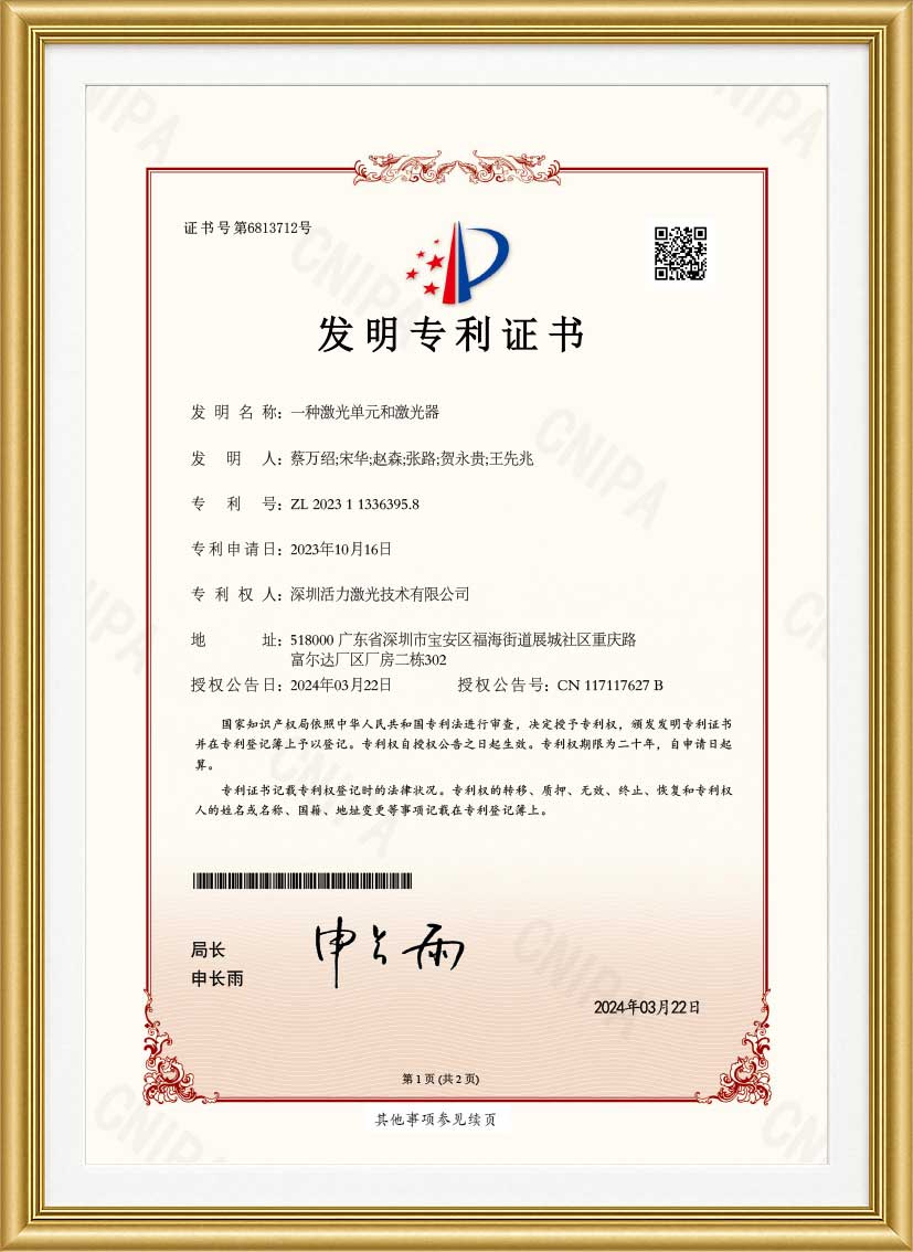
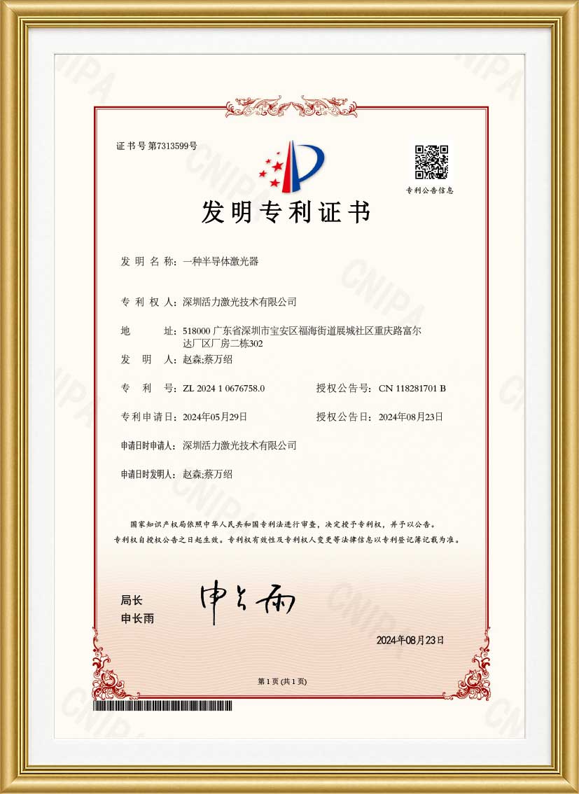
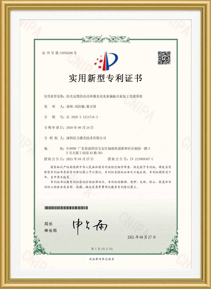
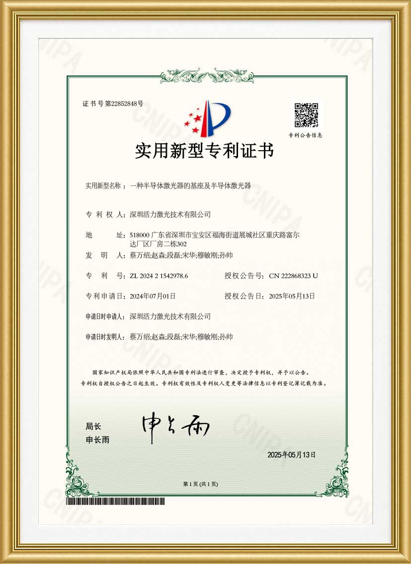
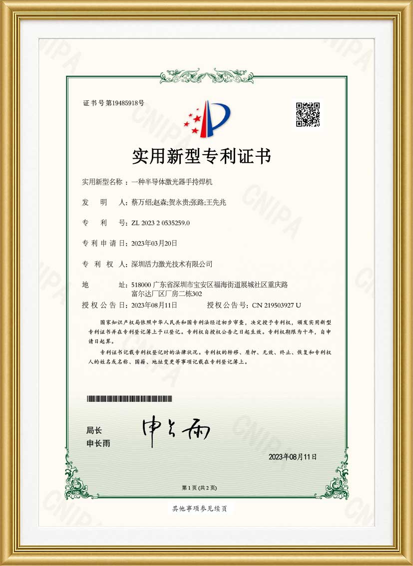
8 invention + 26 utility model patents; participant of the “878 nm High-Power Diode Laser Chip” group standard.
National Certifications & ISO 9001
National High-Tech Enterprise; “Specialized and New” SME; ISO 9001 QMS.
878.6 nm Segment Leader
Market-proven narrow-spectrum 878.6 nm series, first-tier supplier to leading OEMs in the segment; ~30% share in this niche.
Advanced Thermal Management
Design Simulation
Build a multi-scale thermal model spanning chip, package, optics, mechanics, and system. Calibrate 3D FEA with lab data (bulk κ, contact R_th, TIM thickness), validate with prototype temperature curves. Use the model to drive layout, materials, and heat-spreader choices.
Time Scale — Transient Thermal Management
For QCW and power steps, analyze thermal time constants and transient maps down to bar/emitter level. Compute peak junction temperature and recovery to set current slew limits, add thermal mass/diffusion layers, and synchronize cooling control.
Time Scale — Steady-State Thermal Management
Under CW, radial gradients cause thermal crosstalk if waste heat is not removed. We tune cold-plate channels and interfaces, add spreading layers and high-κ shunts (على سبيل المثال., diamond composites) to reduce ΔT and crosstalk.
Spatial Scale — Thermal Distribution & Pathing
High-power multi-module stacks need thermal highways. With placement, layering, and guided conduction, we remove hot spots, open main paths, and minimize thermo-mechanical drift that hurts optical alignment.
Real-Time Thermal Monitoring Toolkit
Use IR thermography, micro-thermocouples, and embedded sensors to build production thermal maps. Feed data back to the model to keep simulation aligned with manufacturing.
Beam-Shaping
Next-Gen Packaging Materials (with κ Ranges)
Legacy CuW (~180–220 W/m·K) and AlN composites (~170–250 W/m·K) limit further scaling. We adopt SiC (~450–480), Al-diamond (~400–500), Cu-diamond (~450–600), Ag-diamond (~800–900), poly-diamond (~1200–2200), and mono-diamond (>2200), matching CTE to target stacks for higher power margins.
Process Optimization: Reflow / Au Wire Bond / Interconnect
We minimize voids and residual stress via vacuum reflow (profile & flux control), stabilize Au wire bonds with tuned ball-wedge, ultrasonics, and force windows, and optimize interconnect routing/vias/relief zones to remove thermo-mechanical stress concentrators.
Structural Optimization: Sequence / Layering / Constraints
We tune assembly sequence and layer thickness, add isolation layers and constraint ribs to dissipate stress without harming optics or thermal paths. Torque/displacement SPC limits lot-to-lot variance, and stress checkpoints are part of mass-production sampling.
Power Integration & Efficient Fiber Coupling
Single-Emitter Power Integration
A single-emitter diode is the smallest optical unit. Using a standardized chain—shaping → collimation → (SBC/PBC/WBC/ECFWBC) combining → re-collimation → fiber coupling—we low-loss combine tens to hundreds of emitters into the same aperture, scaling from hundreds of watts to kW-class. This route offers intuitive alignment, controlled tolerances, and service-friendly maintenance, ideal for incremental scaling and fast field replacement. When tighter spectral quality is required, ECFWBC can be added to narrow linewidth and improve channel uniformity.
Line-Array Combining
A line-array diode laser uses the bar as the smallest module and stacks multiple arrays in space to synthesize power, with optional stacked-bar stages to reach kW to tens-of-kW output. Line-array combining typically employs conductive or macro-channel heatsinks and optically adds power from separate spatial positions. Advantages include independent optical paths, simple/high-accuracy alignment, and minimal tolerance accumulation, plus distributed heat sources that are easier to cool. Arrays are electrically isolated from coolant, allowing the use of purified water, and the collimated beams are not limited by heatsink thickness, yielding no dark zones in the combined spot. The trade-off is footprint: the array layout is more dispersed, so for the same power it is bulkier than stacked-bar designs. Considering footprint and optical complexity, the number of arrays in one combiner is generally kept below ~50, making this route especially cost-effective from hundreds of watts up to ~3 kW.
Stacked-Bar Combining
We tune assembly sequence and layer thickness, add isolation layers and constraint ribs to dissipate stress without harming optics or thermal paths. Torque/displacement SPC limits lot-to-lot variance, and stress checkpoints are part of mass-production sampling.
ECF/VBG Locking
External-cavity Design & Assembly
Co-define grating specs, cavity length, tolerances, and thermal control; maintain sub-degree angular and micron-level positional accuracy; match FAC/SAC and re-collimation so coupling efficiency remains high while locked.
Reliability Topics & Acceleration
Address feedback sensitivity, thermal drift, اهتزاز, and contamination with temperature cycling, power-step, and mechanical-shock matrices; specify lock-hold and fallback conditions and a de-lock → auto-relock strategy.
Chip co-design for ECF
Tune facet reflectivity, gain spectrum, and SMSR to balance locking efficiency, slope-efficiency retention, and manufacturability.
Reflected-Light Isolation
Reflected-Light Reuse (Boost Efficiency & Throughput)
Using spatial routing and beam-splitter arrays, we guide the “manageable portion” of back-reflection back into the effective work zone for second-pass utilization. On high-reflectivity metals (Al, Cu), reuse increases incident energy density per unit time and improves throughput. We bound reuse ratios, phase/polarization states, and incidence angles to avoid hot spots and safety risks.
Reflected-Light Recovery (Energy Dissipation & Risk Containment)
For non-reusable reflections, we implement cavity traps / blackbody chambers and absorbers to dissipate or off-axis recover energy, preventing damage to sources and optics. We specify absorber materials, surface textures, and heat paths, packed in shielded / damped housings for long-term stability and easy service.
Reflected-Light Isolation (Feedback Blocking & Safety)
For reflections that propagate back into the source path, we apply polarization-state discrimination and isolation optics (PBS/λ/4, Faraday isolators, PM chains) so forward light passes and return light is rejected. In exposure-sensitive cells, shields/interlocks and power monitors trigger alarms or shutdown when back-reflection exceeds thresholds.
Laser Homogenization
Fiber-Coupled Beam Homogenization
Multiple emitters are shaped, arranged, and coupled into a multimode fiber. Multimode propagation yields uneven energy distribution. We place a fiber-based homogenizer in the coupling chain to equalize the output, delivering a more uniform fiber-end profile, fewer hot spots, and a wider, more stable process window. It aligns with FAC/SAC, collimation, shaping, and combining, enabling replication in production and easy field service.
Array-Spot Homogenization
High-power systems integrate stacked or high-power modules. Stacking gaps and inherent asymmetry often cause non-uniform profiles after combination. With a spot-homogenizer optics set, we segment and recombine the irregular beam to obtain a flatter energy profile within the same aperture. Hot spots and fringes are reduced; near/far-field consistency improves, enabling stable focusing and downstream processing.
Test, Diagnostics & Analytics
Reporting & Traceability
Each lot exports LIV/Spectrum and Near-/Far-Field reports (PDF/CSV) with distributions, limits, outlier flags. Reports include SN/fixture/T-control/operator metadata for end-to-end traceability.
Homogenization Metrics for High-Power Rectangular Spots
We quantify high-power rectangular beams for size, uniformity, and hot spots. KPIs include encircled energy (على سبيل المثال., 95%), uniformity (σ/Δmax), hot-spot peak ratio, and fringe index. These validate fiber-based and array-spot homogenizers and correlate directly with process yield.
Accelerated Life & Reliability Prediction
Full-duty life tests are slow and power-hungry. Our accelerated model uses temperature/current/duty steps plus thermal cycles, damp heat, اهتزاز, shock to reveal infant mortality and slow drift. We decouple early/random/wear-out modes, fit stress-life (S-N) relations, and report B10/B50 with CIs and screening thresholds for production sampling and PPAP-style release.
تكنولوجيا & Innovation
Certified by multiple patents, we deliver innovative and reliable semiconductor solutions trusted by global partners.


Qualifications & Awards
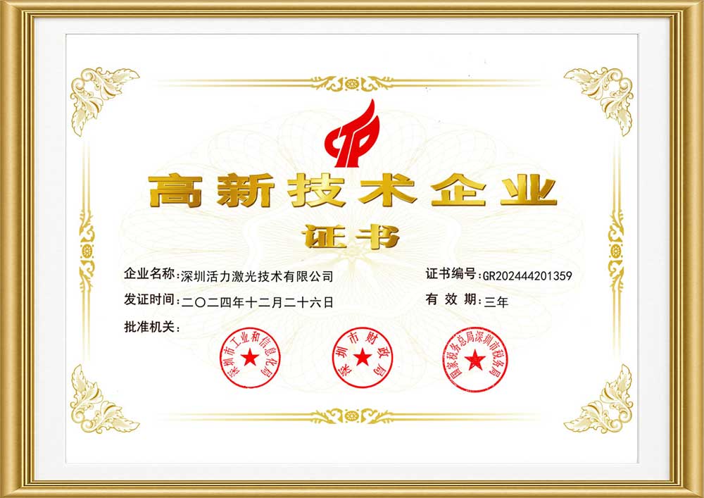
National High-Tech Enterprise Certification

Specialized and Innovative SME Certification
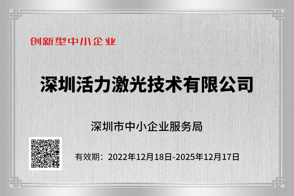
Certification of Innovative SME
.jpg)
شهادة اعتماد نظام إدارة الملكية الفكرية
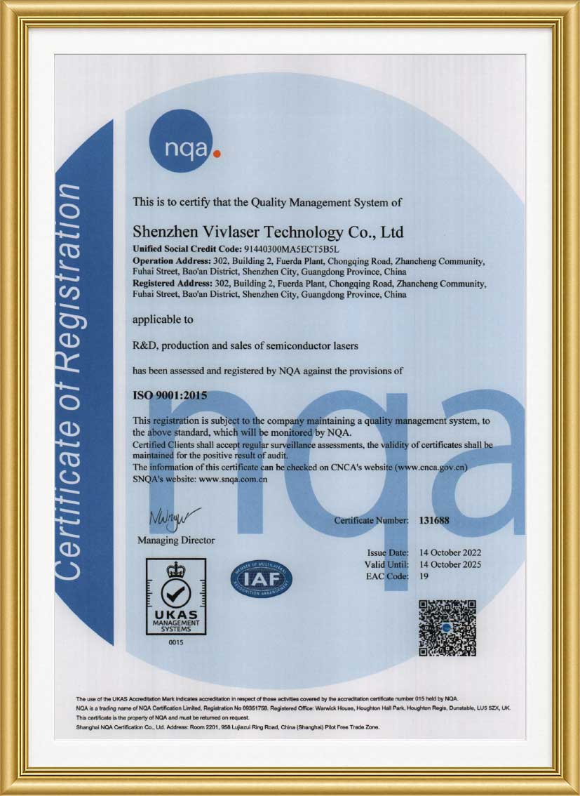
ISO9001 Certificate
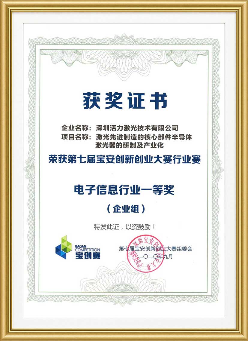
First Prize in the Electronics and Information Sector