Perovskite solar cells reach over 26% efficiency in labs. Yet factories still struggle with stability and speed. Annealing often becomes the hidden bottleneck.
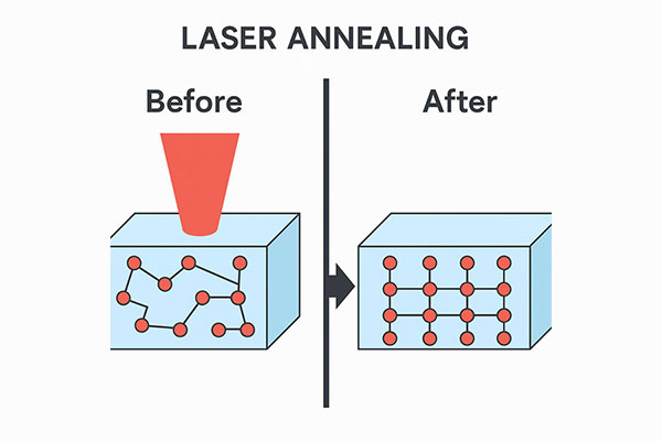
Laser annealing enables rapid crystallization, lower thermal stress, and inline manufacturing compatibility, making it a strong candidate to replace traditional hot-plate annealing in scalable perovskite solar cell production.
Perovskite PV is no longer only a lab topic. It is now a manufacturing question. The real issue is yield, uniformity, and throughput. Annealing sits at the center of this challenge.
Why Does Annealing Matter So Much in Perovskite Thin Films Used in Photovoltaic Devices1?
Many engineers focus on coating. Few fully respect annealing. Yet poor thermal control can destroy an otherwise good film.
Perovskite absorbers are deposited from solution. The wet film must transform into a stable crystalline phase. Annealing drives this transformation.
Annealing removes solvent residues, triggers crystallization, promotes grain growth, and stabilizes the desired perovskite phase. Film morphology after annealing directly affects open-circuit voltage (Voc) and fill factor in solar cells2, recombination losses, and long-term device stability.
Perovskite is not silicon. Silicon uses high-temperature diffusion and well-established crystal control. Perovskite relies on solution chemistry and phase transition dynamics. That makes annealing a primary yield determinant.
How Annealing Influences Device Metrics
| Annealing Factor | Physical Impact | Device-Level Effect |
|---|---|---|
| Temperature ramp rate | Controls nucleation density | Affects grain size distribution |
| Peak temperature | Drives phase transition | Impacts Voc and efficiency |
| Duration | Controls grain growth | Influences fill factor |
| Thermal uniformity | Ensures consistent crystallization | Affects module yield in solar panel manufacturing3 |
Slow heating can promote unwanted intermediate phases. Overheating can cause decomposition. Uneven heating creates performance variation across large modules.
From a manufacturing view, annealing is not secondary. It defines consistency, reproducibility, and module reliability.
Why Is Conventional Thermal Annealing Difficult to Scale?
Hot plates work well in research labs. However, industrial production demands speed and uniformity across large substrates.
Typical lab annealing runs at 100–150°C for 10–30 minutes. This approach is simple. It is also slow.
Conventional hot-plate annealing limits throughput, causes thermal gradients on large substrates, increases thermal stress for flexible modules, and creates challenges for continuous roll-to-roll production lines.
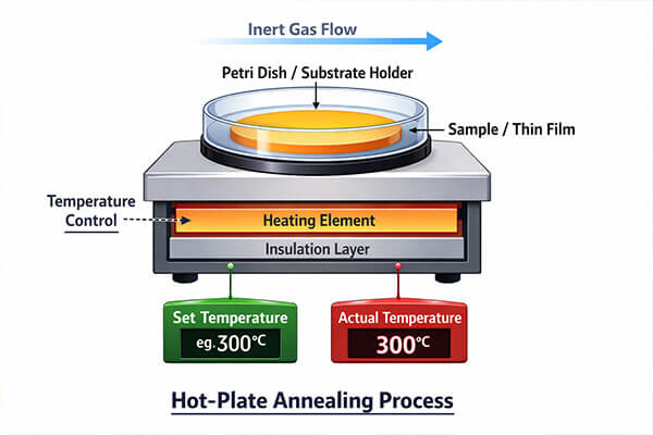
As module sizes grow to square-meter scale, uniform heating becomes harder. Glass shows temperature gradients. Flexible substrates such as PET or PI cannot tolerate long heating above 120°C.
Throughput Constraints
Batch heating creates bottlenecks. If annealing takes 20 minutes, coating speed must slow down. This reduces factory output per square meter.
In gigawatt-scale production, minutes per substrate are too long.
Thermal Budget Limitations
Flexible perovskite modules require low thermal load. Long heating damages polymer substrates and transport layers.
Process Control Challenges
Slow heating affects solvent dynamics. Solvent evaporation interacts with crystallization kinetics. This can lead to:
- Pinhole formation
- Phase segregation
- Non-uniform grain size
Industrial Perspective Comparison
| Parameter | Hot-Plate Annealing | Inline Laser Annealing |
|---|---|---|
| Heating mode | Conduction | Optical absorption |
| Time scale | Minutes | Milliseconds–seconds |
| Thermal load | High | Localized |
| Inline compatibility | Limited | High |
| Flexible substrate support | Weak | Strong |
Industrial scaling requires moving from batch heating to continuous, controllable processing. This is where laser annealing4 enters.
How Does Laser Annealing Change the Thermal Profile?
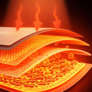
Laser annealing does not heat the entire substrate. It deposits energy directly into the absorber layer.
Laser annealing uses optical absorption5 to create rapid, localized heating in the perovskite layer, enabling high peak temperatures with low overall thermal load and fast cooling rates.

This changes the entire thermal dynamic.
Localized Energy Deposition
The perovskite absorbs laser energy. The glass or polymer substrate remains relatively cool. This reduces mechanical stress.
Rapid Heating and Cooling
Laser exposure can last milliseconds to seconds. The film reaches high surface temperature quickly. After the beam passes, it cools rapidly.
Rapid cooling can influence crystal orientation and defect density.
Thermal Profile Comparison
| Feature | Conventional Heating | Laser Heating |
|---|---|---|
| Heating uniformity | Global | Localized |
| Peak temperature control | Slow | Precise |
| Cooling rate | Slow | Fast |
| Substrate heating | Significant | Minimal |
This profile aligns well with thin-film PV manufacturing. It supports roll-to-roll and tandem integration.
Compatibility with Scalable Systems
Line-beam diode lasers can match slot-die coating width. Scan systems can synchronize with web speed. This allows inline crystallization without interrupting production flow.
At Vivlaser, we understand how beam shaping and wavelength control affect energy distribution. Our experience in high-power semiconductor laser modules6 and wavelength stability supports this type of industrial application.
What Engineering Challenges Must Be Solved?
Laser annealing is powerful. It is also sensitive. It is not plug-and-play.
Laser annealing requires precise control of wavelength, fluence, beam uniformity, and scan strategy. Perovskite materials have a narrow thermal window and can decompose if process parameters drift.
Engineers must design the full system, not just select a laser.
Narrow Thermal Window
Perovskites can decompose above 150–200°C. Excess fluence may cause:
- PbI₂ formation
- Surface roughening
- Organic component loss
Real-time monitoring becomes important.
Wavelength Selection
Absorption depends on wavelength.
- Near-IR (808–980 nm): deeper penetration
- Visible (blue/green): stronger surface absorption
Laser wavelength must match film thickness and layer stack.
Beam Uniformity and Scanning
Large-area modules require:
- Uniform line beams
- Stable overlap
- Controlled scan velocity
Non-uniform energy leads to mixed crystal phases and performance variation.
System-Level Integration
Laser annealing must align with:
- Slot-die coating speed
- Nitrogen atmosphere control
- Real-time feedback systems
This requires integration engineering.
Key Technical Control Points
| Challenge | Risk | Engineering Solution |
|---|---|---|
| Overheating | Film degradation | Fluence optimization |
| Non-uniform beam | Grain inconsistency | Top-hat beam shaping |
| Scan instability | Phase variation | Motion control synchronization |
| Optical mismatch | Inefficient absorption | Wavelength optimization |
High-stability diode laser systems7 with accurate power control are critical. Industrial-grade semiconductor laser modules8 with stable output and fast response help maintain process consistency.
Insight
From my experience with the PV industry perspective, the real battle is no longer record efficiency — it’s LCOE, yield, and scalable throughput. Perovskite has already proven it can compete on efficiency; what it hasn’t proven is that it can run reliably on a gigawatt line with tight process windows and low cost per watt. Annealing sits right in that economic choke point. Traditional thermal methods slow the line, increase thermal stress, and introduce variability across large substrates. Laser annealing, if engineered with industrial-grade stability and beam uniformity, aligns far better with continuous production logic and cost-down roadmaps. In short, for photovoltaics, this isn’t about lab innovation — it’s about whether the process architecture supports bankable manufacturing.
-
Understand material structure and applications ↩
-
Learn key photovoltaic performance metrics ↩
-
See how processing affects production efficiency ↩
-
Explore advanced annealing technology ↩
-
Learn laser-material interaction basics ↩
-
Explore industrial laser technology ↩
-
Understand industrial laser sources ↩
-
Learn about high-power laser modules ↩