<p>Struggling to select the right laser for your solar cell line? A wrong choice can cripple your production yield, leading to costly scrap and downtime.</p>
<p>Selecting the right diode laser for photovoltaic manufacturing involves matching the wavelength, power stability, and beam quality to specific processes like scribing or LFC. Prioritize suppliers who provide long-term reliability data over those who only highlight peak power, ensuring higher production yield and cell efficiency.</p>
<p>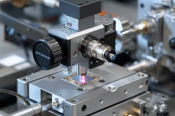 </p>
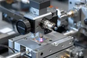
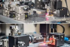
<p>I've spent years helping customers integrate lasers into their production lines. I’ve seen firsthand how focusing only on datasheet specs can lead to trouble. The real challenge isn't finding the most powerful laser, but finding the most reliable one for your specific job. A stable, consistent laser is the foundation of a profitable, high-yield manufacturing process. Let's break down what truly matters when you're making this critical decision.</p>
<p>## How does laser scribing work for thin-film solar cells using P1, P2, and P3 process lines?</p>
<p>Thin-film scribing is a delicate process. Errors in the P1, P2, or P3 scribing steps can create electrical shorts or dead zones, ruining the entire solar module.</p>
<p>Laser scribing for thin-film solar cells uses a sequence of three processes. P1 scribes the top transparent conductive layer, P2 scribes the middle absorber layer, and P3 scribes the bottom metal contact layer. Each step needs a specific laser to isolate cells without damaging adjacent layers.</p>
<p>
</p>
<p>I've spent years helping customers integrate lasers into their production lines. I’ve seen firsthand how focusing only on datasheet specs can lead to trouble. The real challenge isn't finding the most powerful laser, but finding the most reliable one for your specific job. A stable, consistent laser is the foundation of a profitable, high-yield manufacturing process. Let's break down what truly matters when you're making this critical decision.</p>
<p>## How does laser scribing work for thin-film solar cells using P1, P2, and P3 process lines?</p>
<p>Thin-film scribing is a delicate process. Errors in the P1, P2, or P3 scribing steps can create electrical shorts or dead zones, ruining the entire solar module.</p>
<p>Laser scribing for thin-film solar cells uses a sequence of three processes. P1 scribes the top transparent conductive layer, P2 scribes the middle absorber layer, and P3 scribes the bottom metal contact layer. Each step needs a specific laser to isolate cells without damaging adjacent layers.</p>
<p>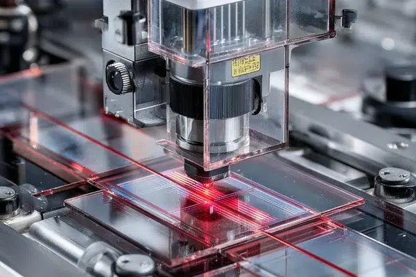 </p>
<p>In my experience, thinking about P1, P2, and P3 as separate, distinct tasks is the key to success. Each step interacts with a different material, so each one needs a carefully chosen laser. You can't use a one-size-fits-all approach here. The goal is complete electrical isolation with minimal collateral damage. The heat-affected zone (HAZ) must be kept as small as possible. If the laser is too powerful or the wavelength is wrong, you can easily damage the layers underneath your target. This creates performance issues that are impossible to fix later. We always advise customers to test lasers specifically for each scribing step.</p>
<p>### Scribing Process Breakdown</p>
<p>| Process Step | Target Material | Goal | Typical Laser Requirement |<br />| :--- | :--- | :--- | :--- |<br />| P1 | Transparent Conductive Oxide (TCO) | Scribe the TCO layer without damaging the glass substrate. | The TCO is transparent to visible light, so a UV laser (~355 nm) is often used for its high absorption. |<br />| P2 | Absorber Layer (e.g., CIGS, CdTe) | Scribe the semiconductor layer down to the TCO layer. | An infrared laser (~1064 nm) works well, as it is absorbed by the absorber layer but not the TCO. |<br />| P3 | Back Contact (e.g., Molybdenum) | Scribe the metal back contact to isolate the cells. | An infrared laser is also effective here, often with short pulses to cleanly remove metal without overheating. |</p>
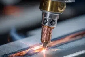
<p>## Why is edge deletion and isolation scribing with diode lasers so critical?</p>
<p>Current leakage at the edges of a solar cell can drastically reduce its efficiency. If the edges are not properly isolated, the cell's performance is compromised, lowering panel output.</p>
<p>Edge deletion uses a diode laser to create a precise groove around the cell's perimeter, removing conductive material. This isolation prevents electrical shunting and leakage currents, which are major causes of efficiency loss. A stable beam ensures a clean, continuous scribe for maximum cell performance.</p>
<p>
</p>
<p>In my experience, thinking about P1, P2, and P3 as separate, distinct tasks is the key to success. Each step interacts with a different material, so each one needs a carefully chosen laser. You can't use a one-size-fits-all approach here. The goal is complete electrical isolation with minimal collateral damage. The heat-affected zone (HAZ) must be kept as small as possible. If the laser is too powerful or the wavelength is wrong, you can easily damage the layers underneath your target. This creates performance issues that are impossible to fix later. We always advise customers to test lasers specifically for each scribing step.</p>
<p>### Scribing Process Breakdown</p>
<p>| Process Step | Target Material | Goal | Typical Laser Requirement |<br />| :--- | :--- | :--- | :--- |<br />| P1 | Transparent Conductive Oxide (TCO) | Scribe the TCO layer without damaging the glass substrate. | The TCO is transparent to visible light, so a UV laser (~355 nm) is often used for its high absorption. |<br />| P2 | Absorber Layer (e.g., CIGS, CdTe) | Scribe the semiconductor layer down to the TCO layer. | An infrared laser (~1064 nm) works well, as it is absorbed by the absorber layer but not the TCO. |<br />| P3 | Back Contact (e.g., Molybdenum) | Scribe the metal back contact to isolate the cells. | An infrared laser is also effective here, often with short pulses to cleanly remove metal without overheating. |</p>
<p>## Why is edge deletion and isolation scribing with diode lasers so critical?</p>
<p>Current leakage at the edges of a solar cell can drastically reduce its efficiency. If the edges are not properly isolated, the cell's performance is compromised, lowering panel output.</p>
<p>Edge deletion uses a diode laser to create a precise groove around the cell's perimeter, removing conductive material. This isolation prevents electrical shunting and leakage currents, which are major causes of efficiency loss. A stable beam ensures a clean, continuous scribe for maximum cell performance.</p>
<p>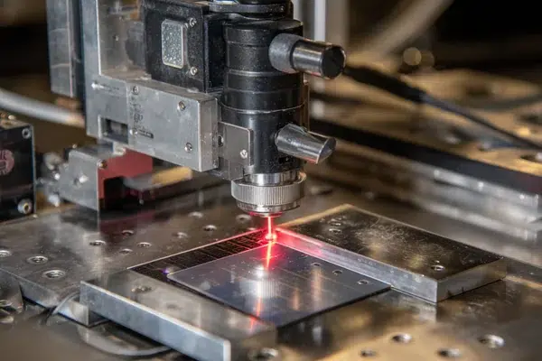 </p>
<p>Think of edge deletion as creating a perfect seal around the active area of your solar cell. Any tiny, leftover conductive path acts like a leak, draining away the power your cell generates. I've seen customers struggle with this when they focus only on the laser's peak power. They run the process fast, but the laser's power fluctuates slightly. These fluctuations create inconsistencies in the scribe. Some parts of the groove are too deep, damaging the silicon. Other parts are too shallow, leaving a microscopic short circuit. The key is not just power, but stable power and excellent beam quality. A high-quality beam (low M²) can be focused to a very fine spot. This allows you to create a narrow, clean isolation trench, maximizing the active area of the cell while ensuring a complete electrical break. This is a classic case where reliability trumps raw power.</p>
<p>### Key Parameters for Edge Deletion</p>
<p> Power Stability: Long-term power stability is non-negotiable. A deviation of even 1-2% can affect the quality of the isolation groove over a large production run, leading to a drop in average cell efficiency.<br /> Beam Quality (M²): A low M² value means the beam can be focused into a smaller, more precise spot. This creates a narrower scribe line, which reduces the "dead space" on the cell and minimizes thermal damage to the surrounding silicon.</p>
<p>## How do Laser-Fired Contacts (LFC) improve PERC solar cell efficiency?</p>
<p>PERC solar cells have a special rear passivation layer that boosts efficiency. But this layer also makes it harder to create the final electrical contacts without causing damage.</p>
<p>Laser-Fired Contacts (LFC) use a pulsed diode laser to locally ablate the rear passivation layer on a PERC cell. This allows the aluminum paste to make contact with the silicon wafer underneath, forming a high-quality electrical connection while preserving the benefits of the passivation layer.</p>
<p>
</p>
<p>Think of edge deletion as creating a perfect seal around the active area of your solar cell. Any tiny, leftover conductive path acts like a leak, draining away the power your cell generates. I've seen customers struggle with this when they focus only on the laser's peak power. They run the process fast, but the laser's power fluctuates slightly. These fluctuations create inconsistencies in the scribe. Some parts of the groove are too deep, damaging the silicon. Other parts are too shallow, leaving a microscopic short circuit. The key is not just power, but stable power and excellent beam quality. A high-quality beam (low M²) can be focused to a very fine spot. This allows you to create a narrow, clean isolation trench, maximizing the active area of the cell while ensuring a complete electrical break. This is a classic case where reliability trumps raw power.</p>
<p>### Key Parameters for Edge Deletion</p>
<p> Power Stability: Long-term power stability is non-negotiable. A deviation of even 1-2% can affect the quality of the isolation groove over a large production run, leading to a drop in average cell efficiency.<br /> Beam Quality (M²): A low M² value means the beam can be focused into a smaller, more precise spot. This creates a narrower scribe line, which reduces the "dead space" on the cell and minimizes thermal damage to the surrounding silicon.</p>
<p>## How do Laser-Fired Contacts (LFC) improve PERC solar cell efficiency?</p>
<p>PERC solar cells have a special rear passivation layer that boosts efficiency. But this layer also makes it harder to create the final electrical contacts without causing damage.</p>
<p>Laser-Fired Contacts (LFC) use a pulsed diode laser to locally ablate the rear passivation layer on a PERC cell. This allows the aluminum paste to make contact with the silicon wafer underneath, forming a high-quality electrical connection while preserving the benefits of the passivation layer.</p>
<p>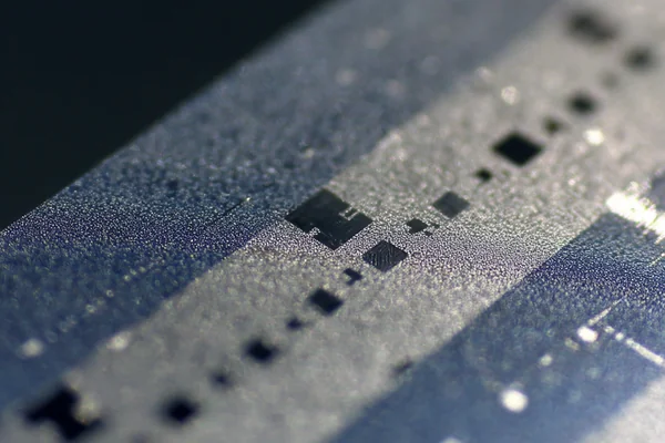 </p>
<p>The LFC process is a perfect example of how lasers enable advanced cell architectures. The entire point of the PERC design is the passivation layer, which reflects unused photons back into the silicon for a second chance at absorption. If you damage that layer during contact formation, you lose the efficiency gain you worked so hard to create. LFC is an elegant solution. It uses a very short laser pulse to open a tiny window in the passivation layer, exactly where the metal contact needs to be. The energy from the pulse is just enough to ablate the thin dielectric layer and melt the aluminum paste above it, which then alloys with the silicon below. The surrounding passivation layer remains untouched. From a product development standpoint, the challenge is delivering a laser with extremely consistent pulse energy and duration. Any variation can lead to either incomplete contact formation or damage to the silicon wafer.</p>
<p>### LFC Laser Requirements</p>
<p> Pulse Control: Short, high-energy pulses (nanosecond or picosecond range) are needed.[^1] This provides enough energy to ablate the passivation layer without conducting significant heat into the bulk silicon, which could create defects.<br /> Wavelength Selection: The laser wavelength must be absorbed by the passivation layer (e.g., SiNx, Al₂O₃) and the metal paste, but not strongly by the underlying silicon. NIR diode lasers (915 nm, 940 nm, 976 nm) are often a good fit for this task.</p>
<p>## Why do different solar cell materials need different laser wavelengths?</p>
<p>Using the wrong laser wavelength is a recipe for failure. It can result in the laser doing nothing at all, or it can cause catastrophic damage to the solar cell.</p>
<p>Different materials absorb light at different wavelengths. For effective laser processing, the wavelength must be strongly absorbed by the target material (e.g., silicon or a metal contact) but transmitted by underlying layers. This ensures precise, localized energy delivery without collateral damage.</p>
<p>A common question I get from procurement managers is, "Which wavelength is best?" The answer is always, "Best for what material?" A laser works by delivering energy in the form of light. If the material is transparent to that light, nothing happens. If it absorbs the light, it heats up. The entire science of laser materials processing is based on controlling this absorption. For solar cells, you are often working with a stack of different thin-film materials. You might need to remove a top layer without touching the one below it. The only way to do that is by choosing a wavelength that the top layer absorbs and the bottom layer does not. That's why our product portfolio includes lasers from the blue spectrum all the way to the infrared. It's not about having options for the sake of it; it's about providing the right tool for a specific material interaction.</p>
<p>### Wavelength Matching for Common PV Materials</p>
<p>| Material | Application Example | Recommended Wavelength & Reason |<br />| :--- | :--- | :--- |<br />| Silicon (Si) | LFC, Laser Doping | ~915-976 nm (NIR): Good absorption in silicon. Cost-effective high-power diode lasers are available. |<br />| Transparent Conductive Oxides (TCO) | P1 Scribing | ~355 nm (UV): TCOs are transparent in the visible/NIR but absorb strongly in the UV, allowing clean removal. |<br />| Metals (Aluminum, Silver, Copper) | P3 Scribing, Contact Firing | ~450 nm (Blue) or ~1064 nm (IR): Metals are highly reflective, but absorption improves at shorter wavelengths. Blue lasers are great for copper[^2], while IR is a workhorse for aluminum. |</p>
<p>## What are the throughput vs quality tradeoffs in high-volume PV manufacturing?</p>
<p>You need to produce millions of cells quickly, but pushing for more speed often hurts quality. Running a laser process too fast can lead to lower cell efficiency and higher scrap rates.</p>
<p>In PV manufacturing, increasing laser scanning speed (throughput) can reduce the energy delivered per unit area. This can cause incomplete ablation or poor contact formation (lower quality). The tradeoff is managed by using higher-power lasers, but this must be balanced with maintaining excellent beam quality and stability.</p>
<p>
</p>
<p>The LFC process is a perfect example of how lasers enable advanced cell architectures. The entire point of the PERC design is the passivation layer, which reflects unused photons back into the silicon for a second chance at absorption. If you damage that layer during contact formation, you lose the efficiency gain you worked so hard to create. LFC is an elegant solution. It uses a very short laser pulse to open a tiny window in the passivation layer, exactly where the metal contact needs to be. The energy from the pulse is just enough to ablate the thin dielectric layer and melt the aluminum paste above it, which then alloys with the silicon below. The surrounding passivation layer remains untouched. From a product development standpoint, the challenge is delivering a laser with extremely consistent pulse energy and duration. Any variation can lead to either incomplete contact formation or damage to the silicon wafer.</p>
<p>### LFC Laser Requirements</p>
<p> Pulse Control: Short, high-energy pulses (nanosecond or picosecond range) are needed.[^1] This provides enough energy to ablate the passivation layer without conducting significant heat into the bulk silicon, which could create defects.<br /> Wavelength Selection: The laser wavelength must be absorbed by the passivation layer (e.g., SiNx, Al₂O₃) and the metal paste, but not strongly by the underlying silicon. NIR diode lasers (915 nm, 940 nm, 976 nm) are often a good fit for this task.</p>
<p>## Why do different solar cell materials need different laser wavelengths?</p>
<p>Using the wrong laser wavelength is a recipe for failure. It can result in the laser doing nothing at all, or it can cause catastrophic damage to the solar cell.</p>
<p>Different materials absorb light at different wavelengths. For effective laser processing, the wavelength must be strongly absorbed by the target material (e.g., silicon or a metal contact) but transmitted by underlying layers. This ensures precise, localized energy delivery without collateral damage.</p>
<p>A common question I get from procurement managers is, "Which wavelength is best?" The answer is always, "Best for what material?" A laser works by delivering energy in the form of light. If the material is transparent to that light, nothing happens. If it absorbs the light, it heats up. The entire science of laser materials processing is based on controlling this absorption. For solar cells, you are often working with a stack of different thin-film materials. You might need to remove a top layer without touching the one below it. The only way to do that is by choosing a wavelength that the top layer absorbs and the bottom layer does not. That's why our product portfolio includes lasers from the blue spectrum all the way to the infrared. It's not about having options for the sake of it; it's about providing the right tool for a specific material interaction.</p>
<p>### Wavelength Matching for Common PV Materials</p>
<p>| Material | Application Example | Recommended Wavelength & Reason |<br />| :--- | :--- | :--- |<br />| Silicon (Si) | LFC, Laser Doping | ~915-976 nm (NIR): Good absorption in silicon. Cost-effective high-power diode lasers are available. |<br />| Transparent Conductive Oxides (TCO) | P1 Scribing | ~355 nm (UV): TCOs are transparent in the visible/NIR but absorb strongly in the UV, allowing clean removal. |<br />| Metals (Aluminum, Silver, Copper) | P3 Scribing, Contact Firing | ~450 nm (Blue) or ~1064 nm (IR): Metals are highly reflective, but absorption improves at shorter wavelengths. Blue lasers are great for copper[^2], while IR is a workhorse for aluminum. |</p>
<p>## What are the throughput vs quality tradeoffs in high-volume PV manufacturing?</p>
<p>You need to produce millions of cells quickly, but pushing for more speed often hurts quality. Running a laser process too fast can lead to lower cell efficiency and higher scrap rates.</p>
<p>In PV manufacturing, increasing laser scanning speed (throughput) can reduce the energy delivered per unit area. This can cause incomplete ablation or poor contact formation (lower quality). The tradeoff is managed by using higher-power lasers, but this must be balanced with maintaining excellent beam quality and stability.</p>
<p> </p>
<p>This tradeoff is the central challenge in scaling up any laser process. Everyone wants higher throughput. The easiest way to get it is to increase the speed of the scanner that directs the laser beam. But if you double the scan speed, you cut the time the laser spends on any given point in half. This means you deliver half the energy, which may no longer be enough to properly ablate the material or form a good contact. The obvious solution is to use a higher-power laser to deliver the same energy in that shorter amount of time. However, this introduces new risks. A higher-power laser running at its limit can suffer from power instability or thermal issues that degrade its beam quality. A fluctuating beam is the enemy of a consistent process. The real solution is a laser that is not just powerful, but designed for industrial stability. It must maintain its power output and beam pointing accuracy hour after hour, even under heavy thermal load. This is where we focus our reliability testing—long-term aging tests that simulate real production conditions.</p>
<p>### Balancing Speed and Quality</p>
<p>1. Define the Process Window: First, determine the minimum energy required per unit area (fluence) to achieve a quality result at low speed.<br />2. Scale Power with Speed: As you increase scan speed to improve throughput, increase the laser power proportionally to maintain the target fluence.<br />3. Monitor for Stability: The critical step is verifying that the laser can maintain its power and beam stability at that higher output level. Ask suppliers for long-term stability data, not just a spec sheet. A laser with superior stability will give you a wider, more forgiving process window at high speeds.</p>
<p>## Conclusion</p>
<p>Choosing the right laser is about managing process risk. Focus on the laser's real-world stability, reliability, and the supplier's application support to ensure high yield in your production.</p>
<p>---</p>
<p>[^1]: "Effect of Tissue Type and Pulse Duration on Thermal Damage", https://pubmed.ncbi.nlm.nih.gov/3367675/. Research on Laser-Fired Contacts shows that using short pulse durations, typically in the nanosecond or picosecond regime, is critical for cleanly ablating the passivation layer while minimizing the heat-affected zone (HAZ) and preventing the formation of crystal defects in the underlying silicon wafer. Evidence role: mechanism; source type: paper. Supports: The claim that short (nanosecond or picosecond) laser pulses are required for the LFC process to avoid damaging the silicon..<br />[^2]: "Blue laser diode (450 nm) systems for welding copper - NASA ADS", <a href="https://vivlasers.com/blue-laser-welding-in-new-energy-battery-manufacturing/">https://vivlasers.com/blue-laser-welding-in-new-energy-battery-manufacturing/</a>. Reflectivity measurements of copper show a dramatic increase in optical absorption at shorter wavelengths, with absorption at blue wavelengths (~450 nm) being an order of magnitude higher than in the near-infrared (~1064 nm), leading to more efficient and stable laser processing. Evidence role: mechanism; source type: research. Supports: The claim that blue lasers are effective for processing copper due to higher absorption..</p>
</p>
<p>This tradeoff is the central challenge in scaling up any laser process. Everyone wants higher throughput. The easiest way to get it is to increase the speed of the scanner that directs the laser beam. But if you double the scan speed, you cut the time the laser spends on any given point in half. This means you deliver half the energy, which may no longer be enough to properly ablate the material or form a good contact. The obvious solution is to use a higher-power laser to deliver the same energy in that shorter amount of time. However, this introduces new risks. A higher-power laser running at its limit can suffer from power instability or thermal issues that degrade its beam quality. A fluctuating beam is the enemy of a consistent process. The real solution is a laser that is not just powerful, but designed for industrial stability. It must maintain its power output and beam pointing accuracy hour after hour, even under heavy thermal load. This is where we focus our reliability testing—long-term aging tests that simulate real production conditions.</p>
<p>### Balancing Speed and Quality</p>
<p>1. Define the Process Window: First, determine the minimum energy required per unit area (fluence) to achieve a quality result at low speed.<br />2. Scale Power with Speed: As you increase scan speed to improve throughput, increase the laser power proportionally to maintain the target fluence.<br />3. Monitor for Stability: The critical step is verifying that the laser can maintain its power and beam stability at that higher output level. Ask suppliers for long-term stability data, not just a spec sheet. A laser with superior stability will give you a wider, more forgiving process window at high speeds.</p>
<p>## Conclusion</p>
<p>Choosing the right laser is about managing process risk. Focus on the laser's real-world stability, reliability, and the supplier's application support to ensure high yield in your production.</p>
<p>---</p>
<p>[^1]: "Effect of Tissue Type and Pulse Duration on Thermal Damage", https://pubmed.ncbi.nlm.nih.gov/3367675/. Research on Laser-Fired Contacts shows that using short pulse durations, typically in the nanosecond or picosecond regime, is critical for cleanly ablating the passivation layer while minimizing the heat-affected zone (HAZ) and preventing the formation of crystal defects in the underlying silicon wafer. Evidence role: mechanism; source type: paper. Supports: The claim that short (nanosecond or picosecond) laser pulses are required for the LFC process to avoid damaging the silicon..<br />[^2]: "Blue laser diode (450 nm) systems for welding copper - NASA ADS", <a href="https://vivlasers.com/blue-laser-welding-in-new-energy-battery-manufacturing/">https://vivlasers.com/blue-laser-welding-in-new-energy-battery-manufacturing/</a>. Reflectivity measurements of copper show a dramatic increase in optical absorption at shorter wavelengths, with absorption at blue wavelengths (~450 nm) being an order of magnitude higher than in the near-infrared (~1064 nm), leading to more efficient and stable laser processing. Evidence role: mechanism; source type: research. Supports: The claim that blue lasers are effective for processing copper due to higher absorption..</p>
<!-- wp:paragraph --> <p></p> <!-- /wp:paragraph -->