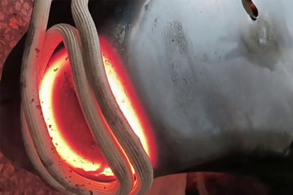
Traditional thermal annealing relies on bulk heating. It’s slow, energy-intensive, and lacks precision—especially problematic for advanced materials and delicate substrates.
Laser annealing offers fast, localized, and precise temperature control, making it the preferred solution for next-generation manufacturing needs.
Conventional heating can’t keep up with modern requirements. As materials and device architectures evolve, the demand for tighter thermal control is accelerating. Here’s why laser annealing is taking the lead.
Where Does Traditional Thermal Annealing Fall Short?
Conventional furnace-based annealing treats the entire material uniformly, regardless of specific processing needs. This leads to high thermal inertia, inefficient energy use, and poor compatibility with sensitive structures.
It struggles with temperature uniformity at micro and nano scales1, causing heat damage, warping, or microcracks—especially in flexible or multilayer substrates.
Key Limitations of Traditional Methods
| Challenge | Description |
|---|---|
| Slow Heat Dynamics | Long ramp-up and cooldown times reduce throughput |
| Lack of Spatial Control | Whole substrates are exposed to unnecessary heat |
| Material Degradation | Delicate layers may warp, crack, or delaminate under uneven stress |
| High Power Consumption | Bulk heating wastes energy |
| Poor Compatibility | Inadequate for ultra-thin or temperature-sensitive materials |
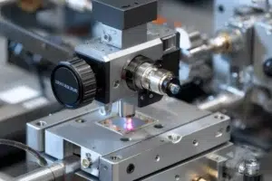
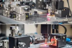
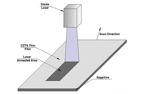
How Does Laser Annealing Deliver Localized Thermal Precision2?
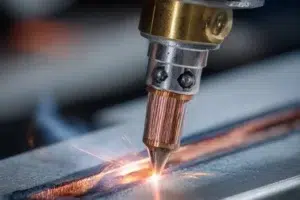
Laser annealing uses tightly focused, high-power beams at specific wavelengths to selectively heat target regions. It enables ultra-fast thermal cycles—often in microseconds.
This minimizes heat-affected zones, reduces stress, and allows fine-tuned control over annealing depth, energy, and duration.
Laser-Based Precision
-
Targeted Energy Delivery: Heats only the areas that need treatment
-
Rapid Thermal Cycling3: Reaches high temperatures quickly and cools down just as fast
-
Programmable Process: Adjustable wavelength, pulse duration, and power for custom profiles
-
Versatile Integration: Ideal for batch, inline, and roll-to-roll processing setups
Which Industries Benefit Most from Laser Annealing?
The ability to apply heat without physical contact and with pinpoint accuracy gives laser annealing a strategic advantage across several advanced sectors.
Semiconductors, displays, and advanced materials manufacturing are leading adopters of this transformative technique.
Key Industry Applications
| Sector | Application Example |
|---|---|
| Semiconductor | Dopant activation, shallow junction repair |
| Display Technology | IGZO or LTPS crystallization for OLED/LCD panels |
| Advanced Metallurgy | Localized hardening and phase transformation |
| Flexible Electronics | Heat-sensitive processing without mechanical distortion |
| Ceramics & Optics | Microcrack removal, structure refinement |
How Do Semiconductor Lasers Drive the Laser Annealing Process?
Semiconductor lasers serve as the light engine of laser annealing systems. Their role is critical in delivering stable, high-intensity, and controllable energy.
The quality of the pump laser4 determines beam stability, annealing precision, and long-term system reliability.

The Role of High-Power Diode Lasers
-
High Power Density5: Delivers sufficient energy within milliseconds
-
Excellent Beam Shaping: Tailored profiles for uniform energy absorption
-
Thermal and Spectral Stability: Maintains performance under extended operation
-
Compact Form Factor: Supports system miniaturization and OEM integration
Why Are Wavelength-Locked Narrow-Spectrum Lasers Essential for High-End Annealing?
Processes like polycrystalline silicon crystallization and IGZO activation demand precise wavelength alignment and minimal spectral drift.
Locked-wavelength, narrow-linewidth lasers1 provide consistent energy delivery and improve material absorption efficiency, crucial for process repeatability.

What Precision Looks Like
-
Spectral Purity: Linewidths under 1nm for accurate thermal coupling
-
Wavelength Stability2: Maintains ±0.5nm across temperature and current variations
-
Power Scaling: 25W to 300W+ modules available for various throughput levels
-
Proprietary Solutions: Vivlaser’s locked 976nm/808nm platforms lead the industry
How Does Vivlaser Help Clients Modernize Their Annealing Processes?
Vivlaser supports clients from proof-of-concept to mass production, offering high-performance laser modules and engineering services that simplify integration.
We deliver customizable, high-reliability solutions with tight wavelength control and thermal consistency—ideal for demanding annealing applications.
Enabling Smart Manufacturing
-
Custom Optical Design: Application-matched beam shapes and energy distribution
-
Mechanical & Thermal Expertise: Design support for better system integration
-
Reliable Supply Chain: Scalable production ensures timely delivery
-
Field-Validated Results: Deployed by leading semiconductor and display manufacturers
Conclusion
Laser annealing eliminates the inefficiencies of conventional thermal processing. With Vivlaser, it becomes a precise, scalable, and production-ready solution for the future of advanced manufacturing.
-
Understanding these challenges can help improve processes and prevent material damage in sensitive applications. ↩ ↩
-
Understanding this concept is crucial for optimizing laser annealing processes and achieving desired material properties. ↩ ↩
-
Exploring this topic can enhance your knowledge of thermal management in laser applications, leading to better results. ↩
-
Understanding the significance of pump lasers can enhance your knowledge of laser technology and its applications. ↩
-
Exploring this topic will provide insights into the efficiency and effectiveness of laser annealing in various applications. ↩